Home | Projects | Notes > Computer Architecture & Organization > Introduction to the Stored Program Machine & ARM
Introduction to the Stored Program Machine & ARM
Introduction to the Stored Program Machine
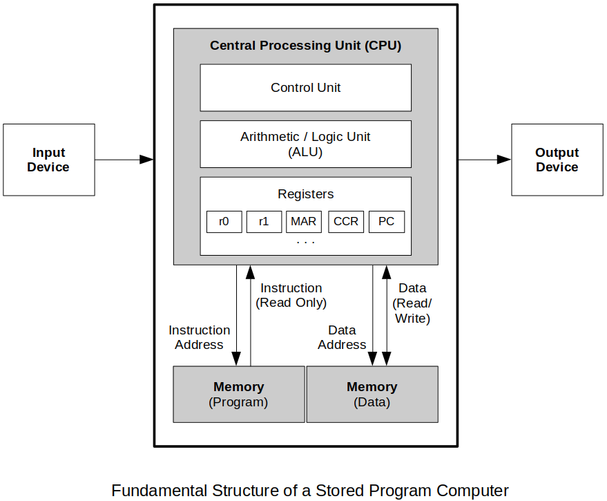
A microprocessor like the ARM has a stored program architecture which, Locates programs and data in the same memory.
Operates in a fetch-execute mode.
Instructions are read from memory, decoded, and executed sequentially.
Such a modern CPU consists of the following major hardware:
Arithmetic and Logic Unit (ALU)
Does unary, binary or ternary operations.
Memory
Registers, Random Access Memory (RAM), Read Only Memory (ROM), etc.
Buses
Allows the trasfer of information from various locations within the CPU, memory, I/O devices, etc.
Control Unit
Based on the instruction and addressing modes, sends signals to the registers, ALU, buses, memory, I/O devices to execute the instruction.
In general, the most sophisticated component of all.
Connected to the most of the important components inside the CPU.
Registers
Register have names rather than addresses.
ARM register:
r0,r1,r2, ... ,r15Intel registers:
AX,BX,CX,DX,SP,BP,SIFreescale registers:
D0,D1, ... ,D7
Categories of registers
General purpose registers
Hold the temporary data while performing different operations.
Can be accessed/used by the programmers.
e.g.,
r0can be used by the programmer to store any data type or address.e.g., Accumulator, BX, etc.
Special purpose registers
Hold the status of a program and are designated for special purpose.
Cannot be directly accessed by the programmers, but can be controlled by the programmers only by the execution of branch instruction.
e.g., Stack Pointer (SP), Program Counter (PC), Condition Code Register (CCR), etc.
Invisible registers
Needed by the CPU but cannot be direcly accessed or controlled by the programmer.
e.g., Instruction Register (IR), Memory Address Register(MAR), Memory Buffer Register (MBR), etc.
ARM
ARM Registers (Not the whole truth but good enough for now)
Program counter (PC)
Contains the address of the next instruction to be fetched from memory.
Instruction Register (IR)
Contains the current instruction being executed.
The instruction is decoded and the control signals are generated to execute the instruction.
Memory Address Register (MAR)
Contains the address of the data that is being read from or writtne to memory.
Memory Buffer Register (MBR)
Contains the data that is being read from or written to memory.
MAR and MBR works in conjunction with each other.
Condition Code Register (CCR)
Contains bits that show the results of the ALU calculations.
In case of the ARM:
Z(Zero),N(Negative),C(Carry),V(Overflow).
r0 ~ r15
A set of 16 registers that store data.
ARM Instruction Formats
Some RISC machines (e.g., ARM, PowerPC, MIPS, etc.) are called load-store machines in that they have only two instructions to access memory; one to read from memory, and the other to write to memory. All other instructions are ALU operations related which only occur between registers.
Two categories of instructions in a load-store architecture
Memory access
Memory to Register:
LDR(Load Register)Register to Memory:
STR(Store Register)
ALU operations
Register to Register:
operation <Reg destination>, <Reg source1>, <Reg source2>
Limiting operations only to registers greatly simplifies the hardware of the CPU but more instructions have to be written by the programmer to get the same effect.
General format of the assembly instructions for the ARM
xxxxxxxxxx11<label>: <instruction> <operand1>, <operand2>, <operand3>Example: A three-operand instruction.
xxxxxxxxxx121LDR r0, 1234 (Takes the contents of memory location 1234 and loads the2value into r0)3[R0]←[1234] (RTL notation)45STR r1, 3456 (Takes the contents of r1 and stores the value into memory6location 3456)7[3456] ← [r1] (RTL notation)89ADD r1, r2, r3 (Takes the contens of r2 and r3, adds them together and10stores the results into r1. r2 and r3 remain unchanged)1112[r1] ← [r2]+[r3] (RTL notation)First two instructions (
LDR..., STR...) are direct addressing modes; The effective address is contained in the instruction register. (ARM does not support direct addressing mode but almost every other processor does.)Again, since ARM does not support direct addressing, operands have to be preloaded into the registers for the operations to be performed.
Control signals from the control unit to execute the instruction:
xxxxxxxxxx31Bus P ← [r2];2Bus Q ← [r3];3[r1] ← ADD(P, Q);
Structure of a Hypothetical Stored Program Machine
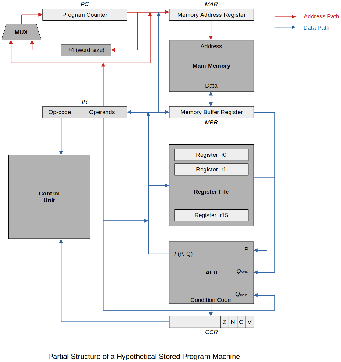
Address bus is share by:
The Program Counter (PC)
Memory Address Registers (MAR)
The Operands part of the Instruction Register (IR)
Data bus is shared by:
The Operands part of the IR
The ALU
Once something goes out to the bus then nothing else can be put on the same bus until the next time slot. The next time slot or clock pulse will clear the current control signals.
Notes about the diagram
The control unit has connections to every component of the CPU. For simplicity these connections are NOT shown on this diagram.
Address bus (red arrows) is all the buses connected to the MAR and PC.
Data bus (blue arrows) is all the buses connected to the MBR, registers and ALU.
Each register has a read from bus and an out to bus signals.
IR has both out to data bus and out to address bus.
A memory read looks like:
[MBR] ← [[MAR]]A memory write looks like:
[[MAR]] ← [MBR]Q[MBR]-[MBR]is invoked when the contents of the MBR are used. Otherwise,Qwill be one of the registers.f(P, Qx)is the function that controls the ALU. Examples:ADD(P, Q)- Adds the values of what is on busPandQand puts the results out on the ALU output bus.Xfer(P)- Trnsfers the contents of busPto ALU output bus.SUB(P, Qliteral)- Subtracts the value of literal part of the IR from what is on busP.
Instruction Fetch
All stored program machines have to go through the exact same instruction fetch process.
ARM instruction fetch process using the register notation:
xxxxxxxxxx171FETCH2-----3[MAR] ← [PC] : Get ready to fetch the next instruction from memory.4[PC] ← [PC] + 4 : Point to the next instruction; 4 is word size. (Good time5to do this since reading from memory takes relatively6long time.7[MBR] ← [[MAR]] : Read the instruction from memory and store results.8[IR] ← [MBR] : Transfer the instruction to the instruction register9and start the decode process.1011LDR (This is a 'direct addressing' example. ARM does not support this mode.)12---13[MAR] ← [IR(address part)] : Copy the operand address from IR to MAR.14[MAR] ← [[MBR]] : Read the data from memory and store results.15[rX] ← [MBR] : Move the data (operand) to rX through the data bus.16Because of the way the control unit works with the IR, a17register rX do not need to be specified.
Literals
Note for this section that the ARM does support literal addressing and does NOT support direct addressing. The syntax given here for direct addressing is for illustration purposes only and cannot be used in your ARM assmbly programs. Other processors do support direct addressing and that is why direct addressing is being discussed in this section.
Direct Addressing Mode
Address field in the instruction contains the effective address of the operand and no intermediate memory access is required.
Example
xxxxxxxxxx31LDR r1, 1234 : Get the data from memory location 1234 and take those2contents and put them into r1.3[r1] ← [1234] : RTL notation.
Literal Addressing
Instead of the instruction pointing to the location of the data, the instruction contains the data. (No effective address but the data is part of the instruction.)
With literal addressing a
#is used to mark the addressing mode as literal.Example
xxxxxxxxxx41LDR r1, #200 : Load 200 into r1. (This does not work on ARM assembly2since LDR and STR require access to a memory location.3Must use the MOV instruction.4MOV r1, #200 : This is the correct syntax for the ARM assembly.Literal addressing saves a memory access so they run faster.
Literal addressing can be used in other instructions:
xxxxxxxxxx21ADD r0, r2, #50 : Add contents of r2 and the literal 50 and store the2reult into r0.
Size of a literal
Since the data is part of the instruction, there has to be a limit on the size of the literal.
In the case of the ARM it is a 12-bit unsigned integer. (The real truth will be covered in the later section.)
212= 4096is the limit.xxxxxxxxxx21LDR r2, #-20 : Not allowed.2LDR r8, #5000 : Not allowed.If you want to subtract with literal addressing you have to use the subtract instruction.
xxxxxxxxxx11SUB r2, r3 #34
In some assemblers, if the literal is not valid (too big) it will automatically define a memory location for you and assign the value to that location.
The instruction is also changed from literal addressing (
MOV) to direct (LDR).
The literal has to be the last operand of the assembly instruction.
xxxxxxxxxx11SUB r1, #56, r2 : Not allowed. The assembler will give error message.Details on LDR
xxxxxxxxxx11MOV r1, #200Control signals (2 ways):
xxxxxxxxxx211. `IR` operand field(`11-0`), literal, out to data bus, instruct `r1` to read that value in.22. Or, `IR` operand field(`11-0`), literal, out to data bus, `ALU` reads in the value through `Q`<sub>`literal`</sub>, instruct the `ALU` to transfer `Q`<sub>`literal`</sub> out to the data bus (`Xfer(Q`<sub>`literal`</sub>`)`), instruct `r1` to read that value in.[!] Note: Follow these two paths on the diagram.
Details on ADD
xxxxxxxxxx11ADD r0, r2, #50Control signals:
IRoperand field(11-0), literal, out to data bus, contents ofr2out to data bus,ALUreads in those two values throughQliteralandP, respectively, instruct theALUto add those two values, put the result tor0.
Some Instructions (Step Through the Flow)
For this example assume the addressing mode is direct addressing. Make sure to understand exactly how the information is passed through and around the CPU. It is also important to know how these control signals change based on different addressing modes.
xxxxxxxxxx601LDR r0, address : Takes the contents of memory location at address and2copies it to r0.3This is direct addressing which the ARM does not support.45[MAR] ← [Operand field of IR; address] IR out to data bus6[MBR] ← [[MAR]] (Read memory)7[R0] ← [MBR] (Or, to make use of ALU, use Xfer(Qmbr))89STR r0, address : Takes the contents of r0 and copies the value to memory10location address.11This is direct addressing which the ARM does not support.1213[MAR] ← [Operand field of IR; address] IR out to data bus14[MBR] ← [R0] (Or, to make use of ALU, use Xfer(P))15[[MAR]] ← [MBR] (write to memory)1617ADD r0, r1, r2 : r0 ← r1 + r2 (r1 and r2 remain unchanged.)1819Bus P ← [R1]20Bus Qmbr ← [R2]21[R0] ← ADD(P, Qmbr)2223[!] Note: Bus choices for r1 and r2 can be changed.2425SUB r0, r1, r2 : r0 ← r1 - r2 (r1 and r2 remain unchanged.)2627Bus P ← [R1]28Bus Qmbr ← [R2]29[R0] ← SUB(P, Qmbr)3031[!] Note: Bus choices for r1 and r2 can be changed.3233BPL target : Branch on positive to location target.34If the result of the previous operation was positive or35zero then go to location target and start program36execution there.37If the result was negative then the next instruction38after the BPL will be executed.3940If CCR (Z and not N)41then [PC] ← [IR 23-0] out to address bus4243[!] Note: When it comes to branching, more portion of the44IR gets involved (i.e., bit 0-23)4546BEQ target : Branch equal.47If the result of the previous operation was zero then go48to location target and start program execution there.49If the result was not zero then the next instruction after50the BEQ will be executed.5152If CCR Z then [PC] ← [IR 23-0] IR out to address bus5354[!] Note: When it comes to branching, more portion of the55IR gets involved (i.e., bit 0-23)5657B target : Unconditional branch.58Go to location target and start program execution there.5960[PC] ← [Operand field of IR; address] IR out to address bus
Hardware Considerations
Since the data is contained in the instruction, there has to be hardware which can put that part of the instruction register (
IR) onto the bus so it can be transferred around the processor and used for calculation.The
IRdecoder has to recognize the addressing mode then have the hardware to only put that constant on the bus to do the operations.Note the 32-bit instruction or 32-bit data from memory is much larger than the number of bits for the literal addressing. The high order bits have to be set to
0.
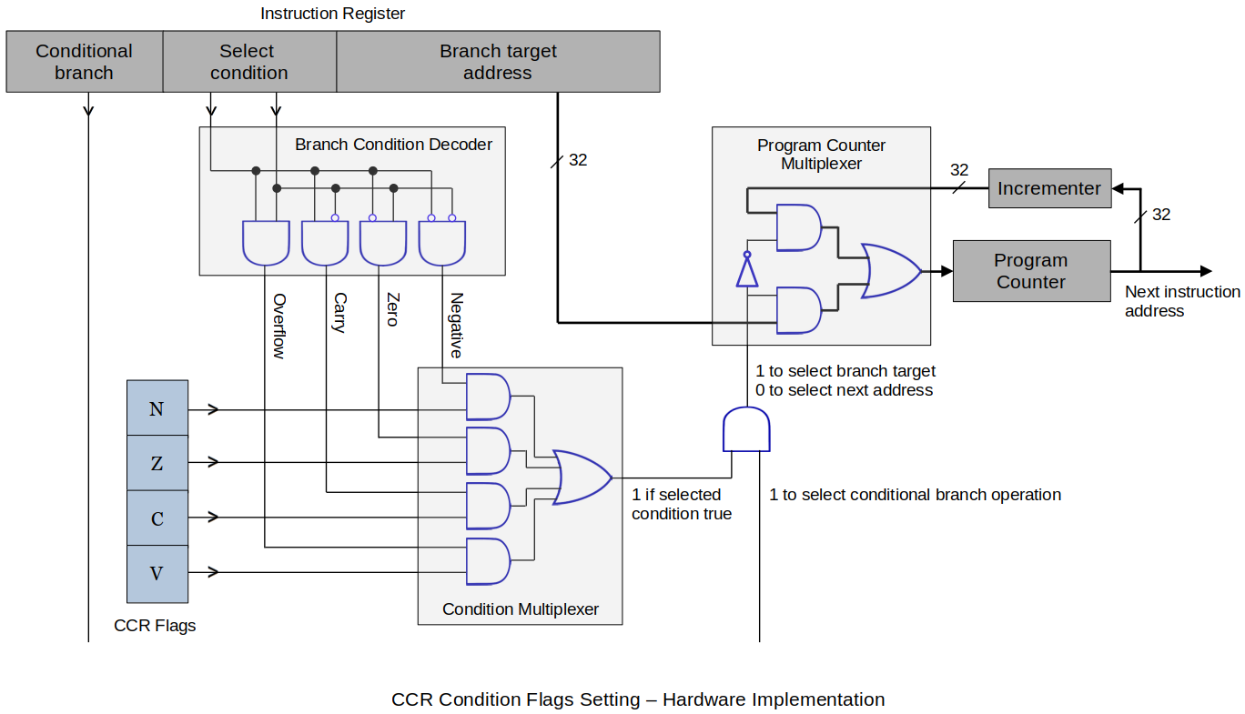
Flow Control
Flow control is the ability to do comparisons and alter the execution sequence based on the results.
It is one of the most important characteristics of a computer.
Conditional Behavior
Based on a calculation or the value of a register branch or do not branch to a certain location.
The
Sat the end of the instruction sets the flags in the Condition Code Register (CCR).Sis optional. If not used,CCRflags will not be set.
Example
xxxxxxxxxx81SUBS r5, r5, #1 : Decrement the loop counter.2BEQ onZero : When the counter hits zero exit the loop.34if notZero, then ADD r1, r2, r35if onZero, then SUB r1, r2, r367[!] Note: onZero is the Branch Target Address (BTA). In this case it is much8like an immediate addressing mode in that the BTA is part of the instruction.
Hardware Consideration
It starts with
ALU. Have to have a way to determine and keep the results of the lastALUoperations. The results go into theCCR.Based on the contents of the
CCRmake, or do not make the jump. If the condition is not met we do not have to do anything. (By default the next instruction is executed.)If the branch has to be made, the
PChas to be updated to the location stored in the instruction.xxxxxxxxxx11If CCR(Zero)=1 then [PC] ← [IR 23-0] IR out to address busFollowing is how an
if... thenlooks like in hardware:

Status Information
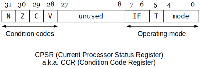
Condition flags (bits)
N: NegativeZ: ZeroC: Carry or borrowV: Overflow
Each of these come from the results of the ALU. They are provided as inputs to the Control Unit.
For the ARM, an "
S" needs to be added to the end of the instruction to get the CCR updated.e.g.,
xxxxxxxxxx31ADDS ...23SUBS ...Or, just use
CMP(Compare) orTST(Test) instruction which forces the CCR update as well.CISC processors (e.g., Intel IA32) update status flags after each operation.
RISC processors, (e.g., ARM) require the programmer to determine when the status flags are updated.
Condition Flags Setting
When the ALU performs an operation, it stores status or condition information in the CCR. The processor records whether the result is:
Negative in two's complement terms (
N),MSB = 1Zero (
Z),all bits = 0Generated a carry (
C), carry out from the full-adder (directly connected toCflag of CCR)Arithmetic overflow (
V)Positive + Positive = NegativeNegative + Negative = PositivePositive(Negative) + Negative(Positive)never produces overflow!
Not all instructions change these bits of the CCR.
Binary Examples Using 8-bit Word
xxxxxxxxxx4110011 0011 512+0100 0010 +663---------- ---40111 0101 117 (correct)56N=0, Z=0, C=0, V=07891111 1111 -110+0000 0001 + 111---------- ---1210000 0000 0 (correct)1314N=0, Z=1, C=1, V=015Zero, Carry1617180101 1100 9219+0100 0001 +6520---------- ---211001 1101 -99 (incorrect)2223N=1, Z=0, C=0, V=124Negative, Overflow(P+P=N)2526271101 1100 -3628+1100 0001 -6329---------- ---3011001 1101 -99 (correct)3132N=1, Z=0, C=1, V=033Negative, Carry3435360000 0000 0000 0000 037-0001 0000 +1111 0000 (two's complement of -0001 0000) -1638---------- ---------- ---391111 0000 -16 (correct)4041N=1, Z=0, C=0, V=0Hardware implementation of condition flags
N:MSBvalueZ: 32 input NOR gateC: Carry out from full-adder directly connected to theCflagV:a(n-1)b(n-1)s(n-1)' + a(n-1)'b(n-1)'s(n-1)meaning,Vflag is set whenP+P=NorN+N=P
Comments about overflows
In C, it keeps on going like nothing ever happened.
In C++, it has the ability to detect and throw an overflow exception. You as a programmer still have to handle it.
In Java, it does not automatically throw an error or overflow exception.
In Assembly, no way! You as as programmer have to check the overflow bit and do all that code yourself.